MANUFACTURE OF PRINTED CIRCUIT BOARDS
M.Manivasagam
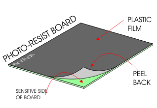 | PHOTO-RESIST BOARD is a piece of glass reinforce plastic. One of the sides is copper clad and this copper has a photosensitive coating. When the plastic film is peeled back this sensitive coating is revealed. After processing this will be the PCB. |
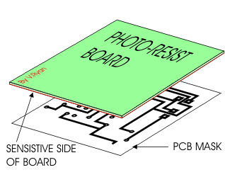 | The PCB mask (now on a transparency) is placed underneath the photo-resist board, touching the sensitive surface. Remember the plastic film must be removed. PCB mask and board are then transferred to the UV light Box. You must be careful to ensure that the PCB mask is the right way up, otherwise when the circuit is etched you will discover that the tracks are also the wrong way round. |
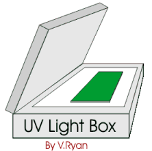 | The lid is shut and the box switched on. The photo-resist board, with PCB mask are left underneath the lid for 2 ½ minutes. The photo-resist board is then placed in a tank filled with developer (using plastic tongs) It is important that the board is only left in the developer for approximately ten seconds. |
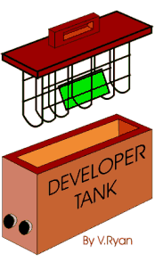 | When the board is taken out of the developer it must be washed in clean water before transferring to the etching tank. Always use plastic tongs. |
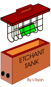 | The etchant is held in a ‘bubble etch tank’ and is heated. This solution slowly etches away the unwanted copper, leaving the tracks only. At this stage it is important to keep checking that the PCB is completed (time - 15 to 45 minutes). If it is left in the tank too long the copper tracks will also be removed or damaged. |
Click Here For Next Page(Final Stage)
Do you have any query or doubts,want to know that PLEASE ask it or leave your ideas at comment..or Just mail me:
MAil Me Your Query or Comments::
Friends,If you find anything incorrect here,PLEASE just inform me,to rectifies it !!!!!!!


0 comments:
Post a Comment